Executive Decision Overview: Semiconductor foundries, fabless microelectronics designers, Tier-1 aerospace electronics manufacturers, and automotive electronic control unit (ECU) integrators face multi-million-dollar field failures, functional safety hazards (ISO 26262), and defense vulnerabilities (DFARS 252.246-7007) caused by remarked, cloned, and harvested microchips. Illicit broker syndicates mechanically blacktop rejected silicon dies, sand down commercial-grade microcontrollers, and apply fake laser markings to re-badge them as military-grade or automotive-qualified ICs. Because electronic packages endure harsh assembly processes—including 260°C lead-free reflow soldering (JEDEC J-STD-020), harsh ultrasonic solvent defluxing, and multi-year thermal cycling (-55°C to +150°C)—traditional packaging labels and external laser text fail to protect active circuit boards. This comprehensive engineering guide examines how sub-micron inorganic covert taggants integrated into Epoxy Molding Compounds (EMC), silicone die potting, and PCB solder mask chemistry deliver permanent, non-destructive, and legally defensible silicon-level verification.
The Global Microelectronics Crisis: Harvested Silicon, Ghost Dies, and Sanded Blacktop Fraud
In high-reliability industrial automation, critical automotive ADAS modules, commercial avionics, and telecommunication infrastructure, integrated circuits (ICs)—including microcontrollers (MCUs), field-programmable gate arrays (FPGAs), power MOSFETs, and analog-to-digital converters—must operate with zero failure across multi-decade lifecycles. High-reliability semiconductors undergo extensive qualification protocols, including AEC-Q100 automotive stress screening, MIL-STD-883 microelectronics testing, and JEDEC moisture sensitivity level (MSL) profiling to eliminate infant mortality and gate oxide breakdown.
However, global electronic supply chain disruptions and extended lead times have created a thriving global black market for fraudulent semiconductors. According to reporting by the Semiconductor Industry Association (SIA) and aerospace defense audit groups, counterfeit microchips infiltrate critical electronic hardware through several sophisticated operational vectors:
- Scrap Harvesting & Lead Re-conditioning: Counterfeiters collect discarded electronic waste (e-waste) circuit boards from scrap processing plants. Workers use propane blowtorches and crude acid baths to desolder surface-mount packages. The extracted ICs undergo lead re-tinning (replacing oxidized solder pins with lead-free alloy finishes), acid-washing to remove thermal burn stains, and re-packaging into carrier tape-and-reel formats. Internally, these harvested silicon dies suffer from severe electrostatic discharge (ESD) micro-fractures, moisture ingress, and damaged bond wires that fail prematurely within hundreds of operating hours.
- Blacktopping & Laser Remarking: Discarded commercial-grade or slower-clock-speed ICs (e.g., consumer microcontrollers rated for 0°C to 70°C) are coated with an ultra-thin layer of black epoxy resin (a process known in the semiconductor industry as “blacktopping”) to conceal existing part numbers. Counterfeiters then use high-precision galvo fiber laser markers to etch the logos, lot codes, and temperature ratings of expensive military-grade (-55°C to +125°C) or high-reliability automotive parts.
- Unauthorized Overproduction & “Ghost Die” Assembly: Outsourced semiconductor assembly and test (OSAT) packaging facilities running authorized production runs frequently package untested, un-diced, or probe-failed “reject dies” harvested from wafer edge trim scrap. These un-passivated ghost dies are packaged into standard plastic packages (QFP, BGA, QFN, SOIC) and sold into secondary distributor broker channels.
When an uncertified clone IC fails in an active flight computer, medical infusion pump, or automotive braking module, equipment manufacturers face massive product liability lawsuits and catastrophic product recalls. Because conventional paper packaging bags and reel barcodes are discarded upon loading onto automated Surface Mount Technology (SMT) pick-and-place feeders, electronics manufacturing services (EMS) providers require direct-on-chip covert forensic authentication integrated into the chemical encapsulation of the semiconductor package.
Why External Laser Text and Acoustic Microscopy Fail In-Line Inspection
Electronics procurement teams and incoming quality control (IQC) laboratories historically relied on visual marking inspection, acetone wipe testing (MIL-STD-883 Method 2009), scanning acoustic microscopy (C-SAM), and destructive decapsulation. Under modern manufacturing throughput, these methods present critical engineering bottlenecks:
- Acetone Resistance of Advanced Blacktopping Resins: Sophisticated counterfeiters no longer use simple lacquer blacktopping that dissolves during a 3-minute acetone wipe test. Modern counterfeit blacktopping utilizes cross-linked cycloaliphatic epoxy formulations cured under heat, rendering the disguise completely impervious to standard solvent wipe tests.
- Destructive Decapsulation Cannot Scale to 100% Volume: Chemical decapsulation (using fuming nitric acid at 90°C to expose the internal silicon die for wafer foundry logo inspection) is inherently destructive. While effective for small sample lots (e.g., 3 units out of a 10,000-unit reel), it destroys the tested component and cannot verify the remaining 9,997 ICs on the active SMT reel.
- Acoustic Microscopy (C-SAM) Throughput Limitations: Scanning acoustic microscopy can detect delamination between the lead frame and epoxy compound, but scanning a single BGA package requires water immersion coupling and takes several minutes per chip. This is completely incompatible with high-speed automated SMT assembly lines placing 40,000 to 80,000 components per hour.
- Laser Serial Cloning: Counterfeiters effortlessly clone genuine OEM laser engraving typography, 2D DataMatrix pin-1 indices, and wafer lot numbers using commercial fiber lasers, making external optical camera inspection completely unreliable for counterfeit detection.
To achieve 100% non-destructive in-line inspection and legal forensic protection, semiconductor foundries and fabless designers must embed covert inorganic crystal taggants directly into the chemical structure of the Epoxy Molding Compound (EMC), liquid potting resins, and PCB solder mask layers.
Epoxy Molding Compound (EMC) & Solder Mask Taggant Chemistry
Mina’s semiconductor anti-counterfeiting architecture integrates sub-micron, thermally stable inorganic rare-earth crystal taggants ($D_{50} < 0.5\ \mu\text{m}$ and $D_{99} < 1.2\ \mu\text{m}$) directly into standard microelectronic encapsulation materials without altering electrical permittivity, thermal dissipation, or moisture sensitivity ratings:
- Epoxy Molding Compound (EMC) Transfer Compounding: During the manufacturing of semiconductor molding compounds (composed of fused silica fillers, biphenyl or o-cresol novolac epoxy resins, and hardeners), covert inorganic taggants are blended at 0.3% to 0.8% by weight. The taggant is homogeneously distributed throughout the solid epoxy pellet. During transfer molding at 175°C (6.0–10.0 MPa), the inorganic particles flow smoothly around microscopic gold, copper, or silver bond wires (wire diameter 15–25 μm) without inducing wire sweep, bond pad cratering, or dielectric voids.
- Liquid Encapsulant & Underfill Potting (Flip-Chip & BGA): Formulated into capillary underfills and liquid epoxy glob-top potting compounds. The sub-micron particle sizing ensures capillary flow under flip-chip dies with bump pitch clearances below 50 μm without particle bridging or localized stress points.
- Liquid Photo-Imageable (LPI) Solder Mask Integration: For printed circuit board (PCB) security, covert taggants are compounded into liquid photo-imageable solder resist inks (green, black, blue, or matte clear). The cured solder mask provides an invisible, permanent cryptographic pattern across high-density interconnect (HDI) circuit boards.
Because the inorganic taggants possess extreme thermal resilience up to 800°C, they are completely unaffected by lead-free reflow soldering profiles (peak temperature 260°C per IPC/JEDEC J-STD-020), wave soldering, and high-temperature operating life (HTOL) burn-in testing.
Technical Comparison: Microelectronics Authentication Solutions
The matrix below compares technical performance metrics across methods used to authenticate integrated circuits and PCB assemblies:
| Technical & Operational Dimension | Surface Laser Marking & Tape Barcode | Destructive Chemical Decapsulation | Mina In-EMC Covert Inorganic Taggants |
|---|---|---|---|
| Non-Destructive 100% Inspection | Non-destructive, but fails to detect blacktopping. | Destructive (destroys the tested component). | 100% Non-Destructive (verified via non-contact optical probe). |
| Resistance to Blacktopping & Sanding | Zero (laser markings sanded off by counterfeiters). | High (exposes inner die), but kills the part. | Immune (taggant is distributed throughout bulk epoxy body). |
| Lead-Free Reflow Soldering (260°C) | Text can oxidize / fade under reflow heat. | N/A (performed offline in lab). | 100% Stable to 800°C (zero degradation during SMT reflow). |
| Impact on Dielectric Constant ($D_k / D_f$) | None. | None. | Zero Impact on dielectric permittivity ($D_k < 3.8$) and loss tangent ($D_f < 0.005$). |
| Inspection Speed on SMT Feeder Line | Requires optical camera focal alignment. | Takes 24–48 hours in chemistry lab. | Instant 0.5s Scan on active tape-and-reel or PCB surface. |
| Legal Proof in Defense & Automotive Audits | Low (disputed due to ease of laser cloning). | Moderate (die photos subject to dispute). | Defensible Spectroscopic Proof of proprietary factory chemistry. |
Electrical, Moisture Sensitivity (MSL) & Outgassing Compliance
In high-reliability semiconductor packaging, any additive introduced into epoxy mold compounds must undergo exhaustive qualification to ensure zero degradation of electrical insulation, thermal dissipation, or moisture sensitivity ratings:
1. High-Frequency Dielectric & Reliability Testing
- Dielectric Constant & Loss Tangent (ASTM D150): $D_k$ remains at 3.6–3.8 at 1 GHz; dissipation factor $D_f < 0.004$, ensuring zero signal attenuation in high-speed 5G RF and radar packages.
- Volume Resistivity (ASTM D257): Maintains $>10^{15}\ \Omega\cdot\text{cm}$ at 25°C and $>10^{12}\ \Omega\cdot\text{cm}$ at 175°C, preventing leakage currents across fine-pitch lead frames.
- High-Temperature Operating Life (HTOL per JESD22-A108): Zero electrical parametric drift after 1,000 hours at 125°C with continuous Vdd bias.
2. Moisture Sensitivity & Thermal Stress
- Moisture Sensitivity Level (IPC/JEDEC J-STD-020): Preserves MSL 1 and MSL 3 ratings (85°C / 85% RH for 168 hours followed by 3× 260°C reflow cycles) with zero package popcorn cracking or internal delamination.
- Highly Accelerated Stress Test (HAST per JESD22-A110): Zero bond pad corrosion after 96 hours at 130°C and 85% RH under electrical bias.
- Total Mass Loss (TML) & Outgassing (NASA SP-R-0022A / ASTM E595): TML < 0.50% and CVCM < 0.05%, meeting strict space-grade vacuum outgassing requirements.
Operational Inspection Architecture: Foundry Lot Allocation, SMT Pick-and-Place, and Field Audits
Deploying covert in-EMC authentication enables semiconductor foundries, electronics distributors, and defense OEM quality teams to establish an unbroken chain of custody:
- Foundry & OSAT Lot Allocation: During semiconductor encapsulation, the molding compound supplier blends proprietary covert taggants with lot-specific spectroscopic keys. The physical batch signature is cryptographically registered to authorized wafer fabrication lots, purchase orders, and OEM customer IDs.
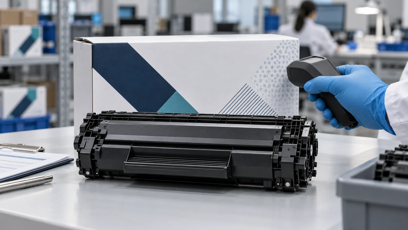
- SMT Feeder Receiving & Tape-and-Reel Intake: When reels of microchips arrive at the EMS factory, receiving technicians swipe a Mina handheld optical scanner across the carrier tape or directly over the molded IC bodies. In 0.5 seconds, the scanner excites the covert inorganic taggants through the transparent carrier tape, verifying genuine foundry origin and flagging cloned blacktopped reels before they are loaded onto automated high-speed SMT pick-and-place feeders.
- Forensic Hardware Audits in Defense & Aerospace Systems: In defense depot overhauls or aviation airworthiness audits, inspectors point the optical probe directly at populated printed circuit boards inside avionics enclosures. The non-contact probe instantly verifies the authenticity of every active processor, memory chip, and voltage regulator without desoldering components or damaging delicate conformal coatings.
Procurement Guidelines: Engineering Due Diligence Checklist
Before standardizing covert taggants across semiconductor encapsulation and PCB solder mask bill of materials, packaging procurement and component engineering directors should verify the following baseline parameters:
Engineering Checklist for Semiconductor Covert Taggant Trials
- EMC Base Chemistry & Filler Loading: Specify exact molding compound grade (e.g., Sumitomo Bakelite EME-G700, Henkel Hysol, or Resonac CEL series) to calibrate inorganic taggant compatibility with high-purity fused spherical silica fillers (filler loading 75%–90% by weight).
- Particle Size Distribution ($D_{50} < 0.5\ \mu\text{m}$): Require laser diffraction particle size reports proving $100\%$ sub-micron dispersion to eliminate wire sweep risks on ultra-fine gold/copper bond wires.
- Thermal Stability at Lead-Free Reflow: Verify that taggant optical emission intensity exhibits zero degradation after multiple 260°C reflow thermal profiles.
- Dual-Custody Supply Chain Security: Enforce ISO/IEC 27001 and ITAR-compliant supply chain custody protocols for delivering covert additive concentrates directly to approved OSAT packaging facilities.
Structuring a 3-Phase Semiconductor Packaging Validation Roadmap
Semiconductor foundries and OSAT packaging partners should execute a disciplined qualification protocol prior to commercial production:
- Phase 1: Laboratory Rheology & Spiral Flow Testing: Compound 0.5% taggant into virgin EMC powder. Measure spiral flow length (EMMI 1-66), gel time at 175°C, melt viscosity, and verify baseline optical excitation response using calibrated spectrophotometers.
- Phase 2: OSAT Assembly Pilot Run (10,000 Molded Packages): Encapsulate 10,000 QFP/BGA packages on industrial transfer molding presses. Conduct X-ray inspection (AXI) and acoustic microscopy (C-SAM) to confirm zero wire sweep, zero internal voids, and verify automated optical reader decodability across various package sizes.
- Phase 3: SMT Lead-Free Reflow & MSL Reliability Trial: Pass marked ICs through 3× 260°C reflow soldering ovens. Execute full electrical parameter testing (ATE test) and subject components to 1,000 hours of Temperature Cycling (-55°C to +125°C per JESD22-A104). Verify 100% optical authentication accuracy after prolonged thermal stressing.
Protect Your Microelectronics Supply Chain from Counterfeit & Harvested Chips
Ensure that every integrated circuit installed in your mission-critical electronic systems delivers genuine foundry reliability and unchallengeable forensic traceability. Consult with Mina’s microelectronics materials specialists to evaluate covert EMC and solder mask formulations and request sample encapsulated test coupons for your laboratory validation.